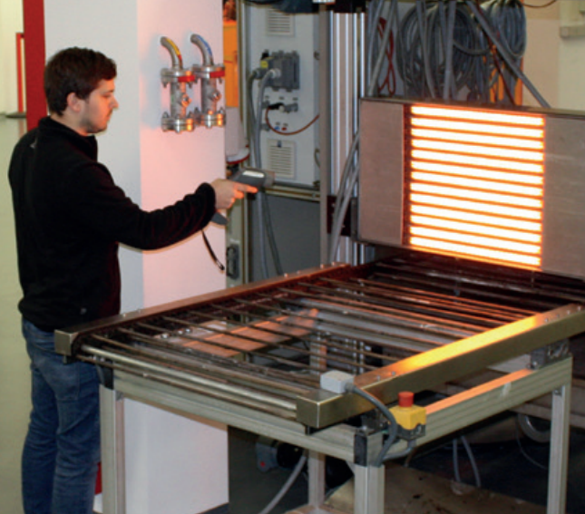
On the line, a wafer’s thermal budget is fixed. One hotspot during burn-in, and the failure mechanism slips into the data instead of getting forced out. We built the wafer burn-in test heating lamp to cut through that ambiguity. What matters under the hood We run near-infrared (NIR) quartz-halogen emitters tuned for fast, directional heat, then close the loop so setpoint stays within ±0.1°C. That keeps wafer-level uniformity on tight thermal profiles without overshoot that can wreck stack layers. The assembly is cleanroom-ready for Class 1–100: low-outgassing materials, sealed junctions, and a particle-controlled design that keeps contamination off the wafer. You get repeatable output, 24/7, backed by documented MTBF and service intervals that keep scheduling uninterrupted. Why this approach fits the process Burn-in and bake steps—soft bake, hard bake, and post-process curing—don’t just need heat. They need repeatable temperature delivery. You end up with consistent line-to-line profiles, less rework, and fewer excursions driven by thermal drift. Energy drops because NIR heats the target directly, and cycle times shorten when ramp-up and cool-down are controlled. In lithography-adjacent work, the same lamp supports photoresist bake windows with tighter margins, improving yield without swapping out your fixtures. What to plan for The lamp performs when the emitter array matches your chuck geometry and thermal mass. Installation hinges on precise optical alignment and verified cooling capacity; if heat removal isn’t there, control bandwidth falls off and uniformity suffers. Commissioning is quick, and from there you get a stable process you can document and keep ready for audits.